In semiconductor industry, Test and Measurement (T&M) instruments are essential for validating the quality, reliability, and performance of semiconductor devices throughout their lifecycle. Extensive testing methodologies are used to identify and address defects, manufacturing variations, and other issues that potentially impact the chip’s performance. Test engineers conduct reliability tests, such as High Temperature Operating Life, Electro Static Discharge, Latch-Up, Temperature Cycling, Thermal aging, and accelerated life testing, to assess how semiconductors perform under extreme conditions and over time.GW Instek test solutions include:
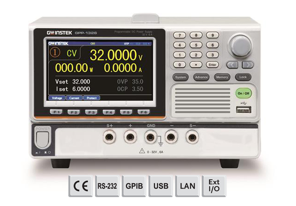
Typical use case example: In MOSFET characterization, a DC power supply biases the gate source and drain source junctions, while measuring the current response.
Suitable for low voltage /low power semiconductor devices
![]()
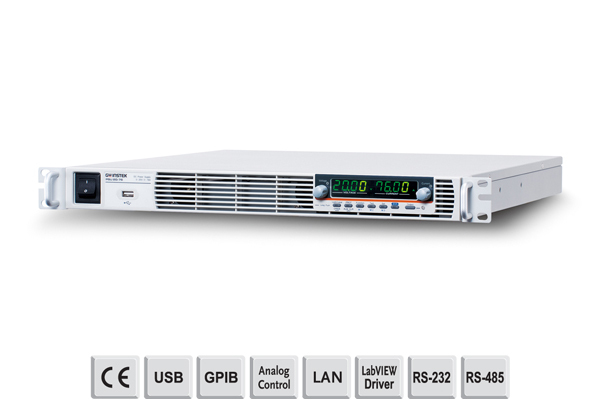
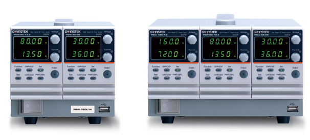
Suitable for high voltage /power semiconductor devices testing for estimating the Switching losses, Efficiency ,studying the thermal behaviour and I-V Characterization.
![]()
Suitable for high voltage /power semiconductor devices testing for estimating the Switching losses, Efficiency ,studying the thermal behaviour and I-V Characterization.

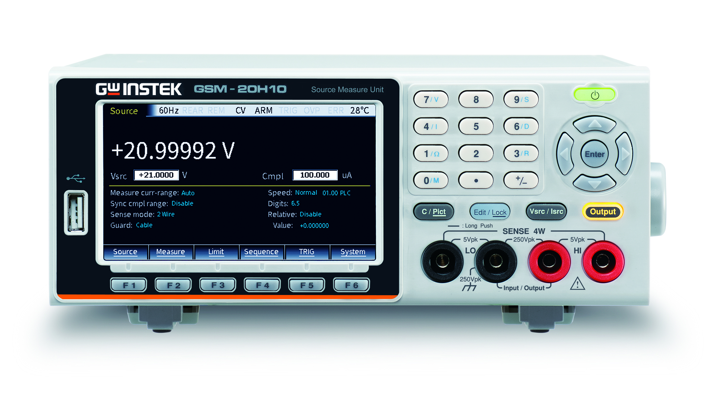
source measure units (SMU) deliver precise voltage and current sourcing with simultaneous measurement capabilities, making them ideal for testing semiconductors, materials , electronic components and I-V characterisation. In The sourcing of voltage and current span across both positive and negative values, SMUs hence have four-quadrant operation while power supplies typically operates in single quadrant.
Key features include:
GW Instek GSM-20H10 is a precision source measure unit that provides highly stable DC power and instrument-grade 6½-digit multimeter measurements.
While operating, this instrument can be used as a voltage source, current source, voltmeter, ammeter, and ohmmeter. GSM-20H10 provides four-quadrant operation of ±210V/±1.05A/22W with an accuracy of 0.012% and a resolution of 1µV/10pA/10µΩ.

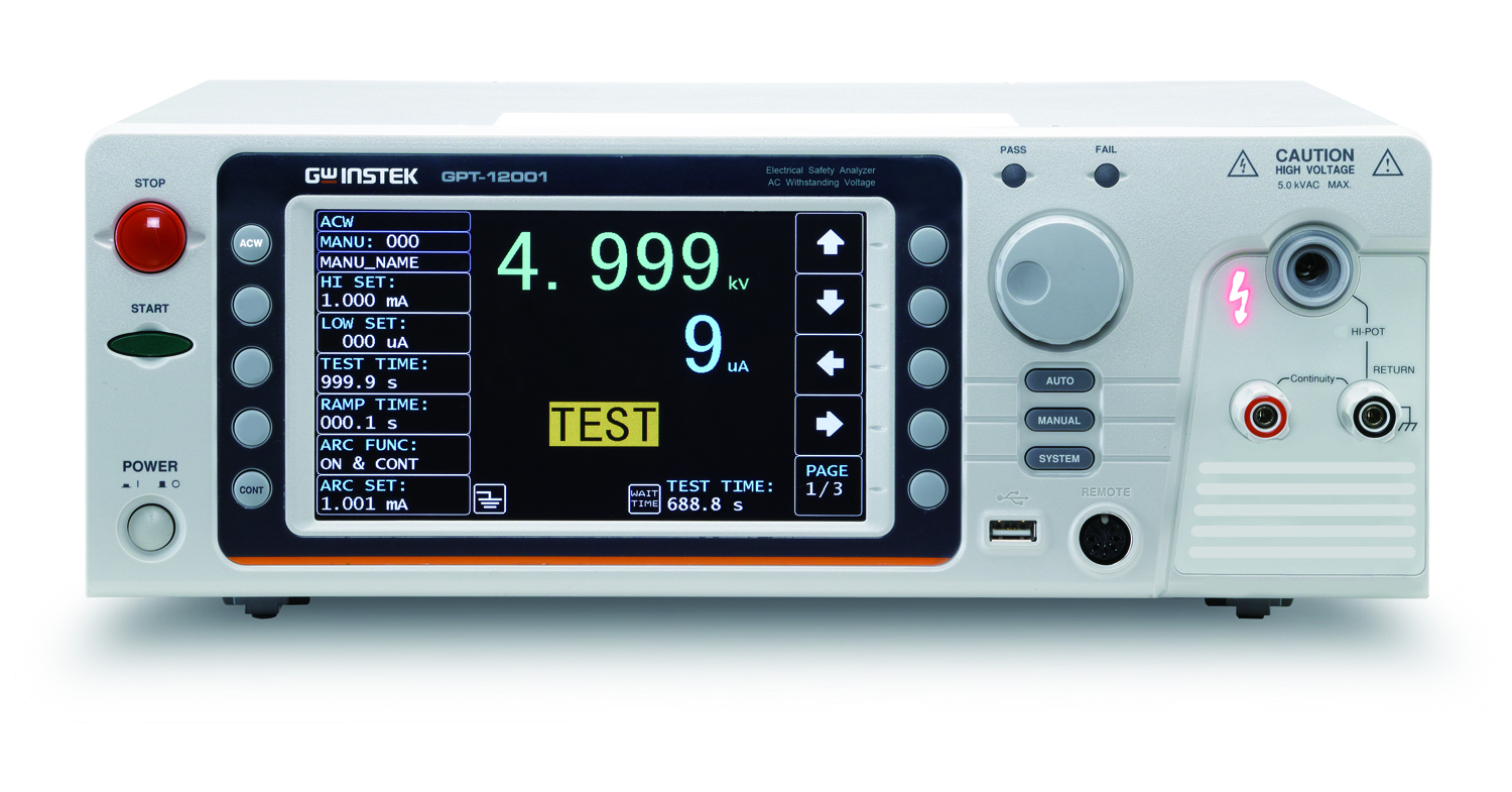
A Hi-Pot (High Potential) Tester is widely used in semiconductor R&D applications to ensure the electrical safety and reliability of devices by testing insulation and dielectric strength. In semiconductor research and development, applications include:

In the semiconductor industry, spectrum analysers are essential for testing RF, analog, and mixed-signal semiconductor devices such as RF transceivers, amplifiers, PLLs, and wireless chips.
Key Applications of Spectrum Analysers in Semiconductor Testing
Bandwidth 9kHz ~ 8.0GHz

Burn-in testing in the semiconductor industry is used to detect early-life failures in chips before they reach the market. The idea is to stress devices under high temperature, voltage, and continuous operation, so that weak or defective units fail in the factory rather than in the field
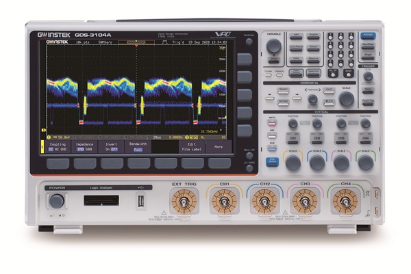
In semiconductor burn-in testing oscilloscopes have critical role for monitoring, debugging, and verifying the devices under stress. They complement the power supplies and electronic loads in the burn-in setup.
Bandwidth -1 GHz

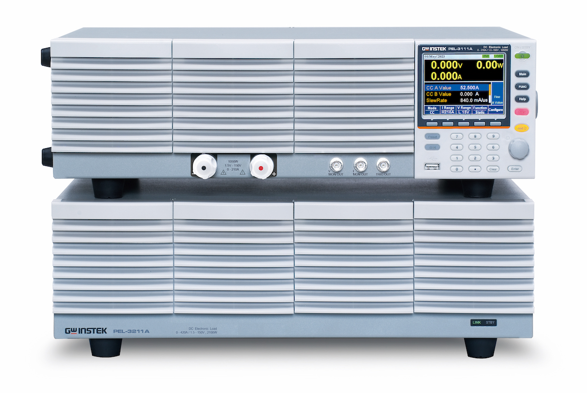
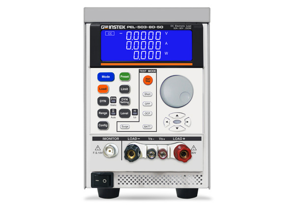
In semiconductor burn-in testing, DC electronic loads are a crucial part of the test setup because they simulate real operating conditions by drawing controlled current from the Device Under Test (DUT). Unlike power supplies, which provide voltage, DC loads pull current in programmable ways to stress the device.


Arbitrary waveform generators (AWGs) are essential for testing mixed-signal Integrated Circuits (ICs) because they provide the flexibility, precision, and high-frequency capabilities needed to simulate complex, real-world operating conditions that standard function generators cannot achieve. Unlike simple signal generators, AWGs can create custom, user-defined waveforms, including modulated signals (QAM, OFDM), noise, and non-standard shapes, allowing for comprehensive validation of both analog and digital circuits on a single chip.
Examples of use cases:
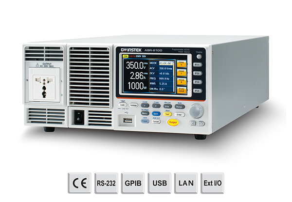
The ASR-2000 series provides users with waveform output capabilities to meet the test requirements of different electronic components /devices. Arbitrary waveform function allows users to store/upload user-defined waveforms and source these waveforms/ signals to their semiconductor devices like mixed signal ICs and setups for testing and validation.
In ASR 2000 series the sequence mode generates waveform fallings, surges, sags, changes and other abnormal power line conditions.

Semiconductor manufacturing and packaging depend on precise, repeatable visual inspection at every stage — from wafer dicing and die placement through wire bonding, flip-chip and wafer-level packaging, to final package inspection and failure analysis. Defects at this scale (broken wire bonds, bump voids, lifted leads, cracked die, contamination) are often invisible to the naked eye but critical to device reliability. Vision Engineering's eyepiece-less stereo microscopes, digital inspection cameras and non-contact 3D inspection systems give process and quality engineers the resolution, depth perception and ergonomics needed for long inspection shifts in cleanroom and lab environments. Vision Engineering Semiconductor inspection solutions include:
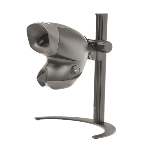
Die attach, wire bonding and wafer handling all require high-resolution stereo viewing with genuine depth perception, since operators must judge wire loop height, bond placement and die tilt in real time. Vision Engineering's eyepiece-less optical design lets inspectors and bond-line operators work through long shifts without the eye strain associated with conventional binocular microscopes.
Typical use case example: During wire bonding, an operator uses a stereo microscope to verify bond placement on the die pad and lead frame, checking loop height and wire dress before the part moves to the next process step.

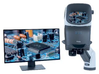
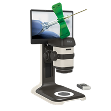
Eyepiece-less stereo microscope for wafer, die and wire-bond level inspection
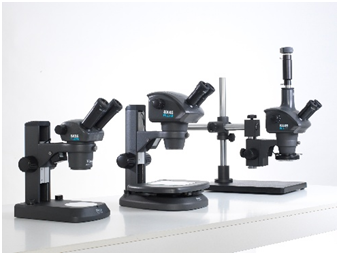
High-magnification stereo microscope for fine-pitch die and bond inspection


General-purpose stereo microscope for incoming wafer and component checks
Flip-chip bumps, wafer-level package (WLP) balls and 3D die-stacking interconnects need non-contact dimensional and coplanarity checks that a 2D image cannot fully capture. Vision Engineering's digital 3D inspection systems display true stereo depth on screen without special glasses, letting engineers evaluate bump height, voiding and surface defects and capture 3D images for process documentation.
Key applications:
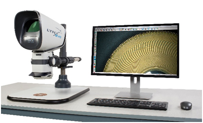
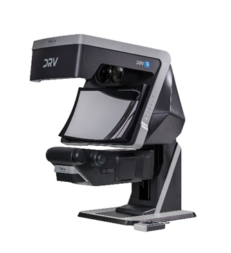
Non-contact 3D inspection for package and die-level dimensional checks

Compact 3D digital microscope for fine-pitch bump and bond inspection
Wide magnification range 3D digital microscope for package-level inspection

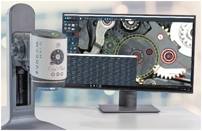
Semiconductor failure analysis labs need high-resolution image capture for defect documentation, decapsulated die inspection and root-cause reporting — often correlating optical images with electrical test data. Vision Engineering's digital microscopes provide 4K/HD image capture with time-stamped reporting for traceable FA records.

4K Ultra HD digital inspection camera for failure analysis documentation
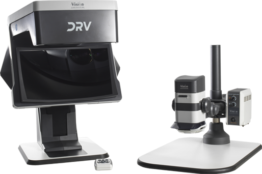
Final package inspection — mould compound quality, lead frame form, marking legibility and singulation — is typically a high-throughput, repetitive visual check. An eyepiece-less viewer removes the need for operators to align their eyes to a fixed eyepiece, speeding up inspection while reducing fatigue on high-volume final-test and packing lines.
Eyepiece-less viewer for high-throughput package and lead-frame inspection
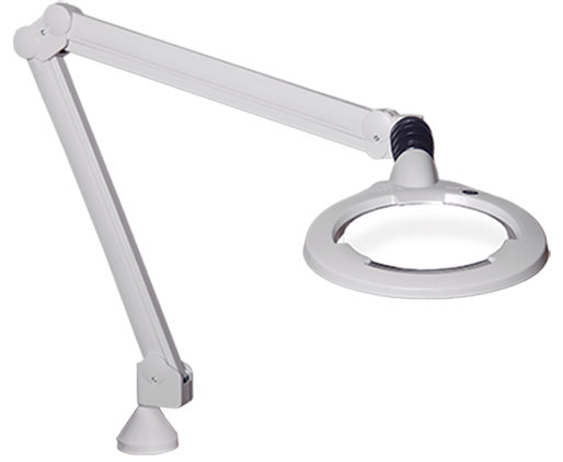
For general wafer handling, die-attach, rework and packing benches inside cleanroom or lab environments, Vision Engineering's illuminated bench magnifiers give shadow-free, glare-free close-up viewing so operators can work accurately at close range for extended periods.

Illuminated bench magnifiers for cleanroom assembly and inspection benches
Image capture directly from the bench magnifier for inspection records

Semiconductor test and assembly environments — test board fabrication, probe card rework, load board assembly, package-level rework and ESD-sensitive lab benches — need soldering tools that combine fine-pitch precision with fast, stable temperature control and ESD safety. JBC's Intelligent Heat Management delivers instant heating when a tool is lifted from its stand and fast temperature recovery during use, protecting sensitive semiconductor test boards and components from thermal stress while keeping tip life long and rework consistent. JBC Semiconductor soldering and rework solutions include:
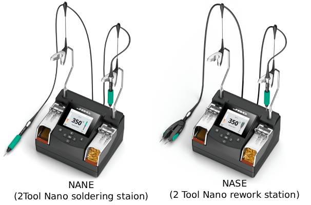
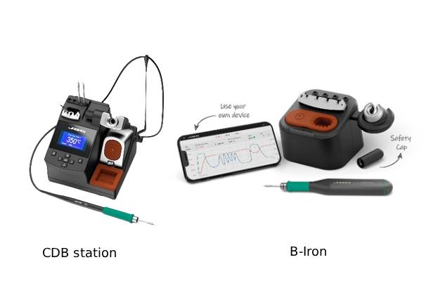
ATE load boards, probe cards and device interface boards carry dense, fine-pitch components and controlled-impedance traces that require precise, low-thermal-stress soldering. JBC's Nano and Compact stations give test-engineering and prototype labs fast, stable temperatures for reliable joints without damaging sensitive board materials or nearby components.
Typical use case example: During load-board assembly, a technician uses a Nano station to hand-solder fine-pitch decoupling components and test points without disturbing adjacent SMD parts or the board's controlled-impedance layers.
Nano Stations
Soldering and rework for the smallest SMD components on test and probe boards
General-purpose soldering stations for test-board fabrication and lab benches
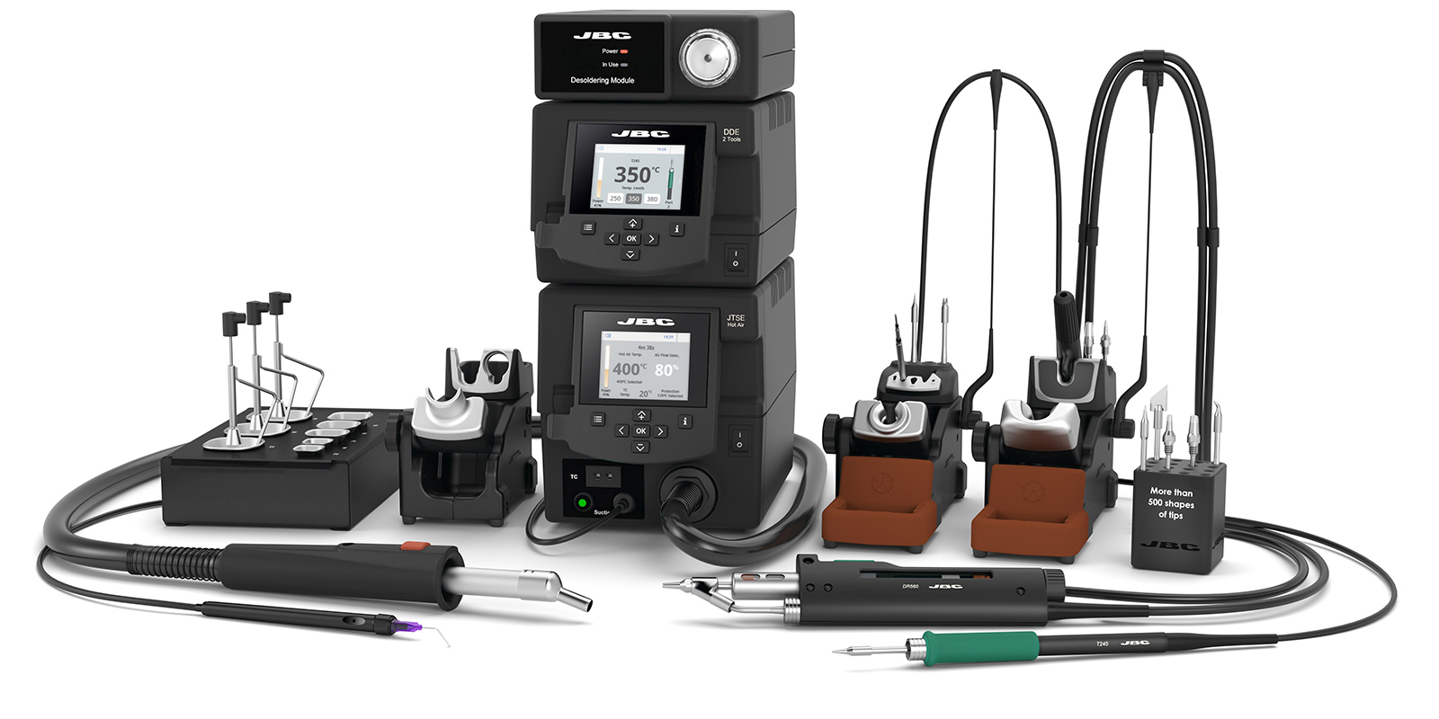
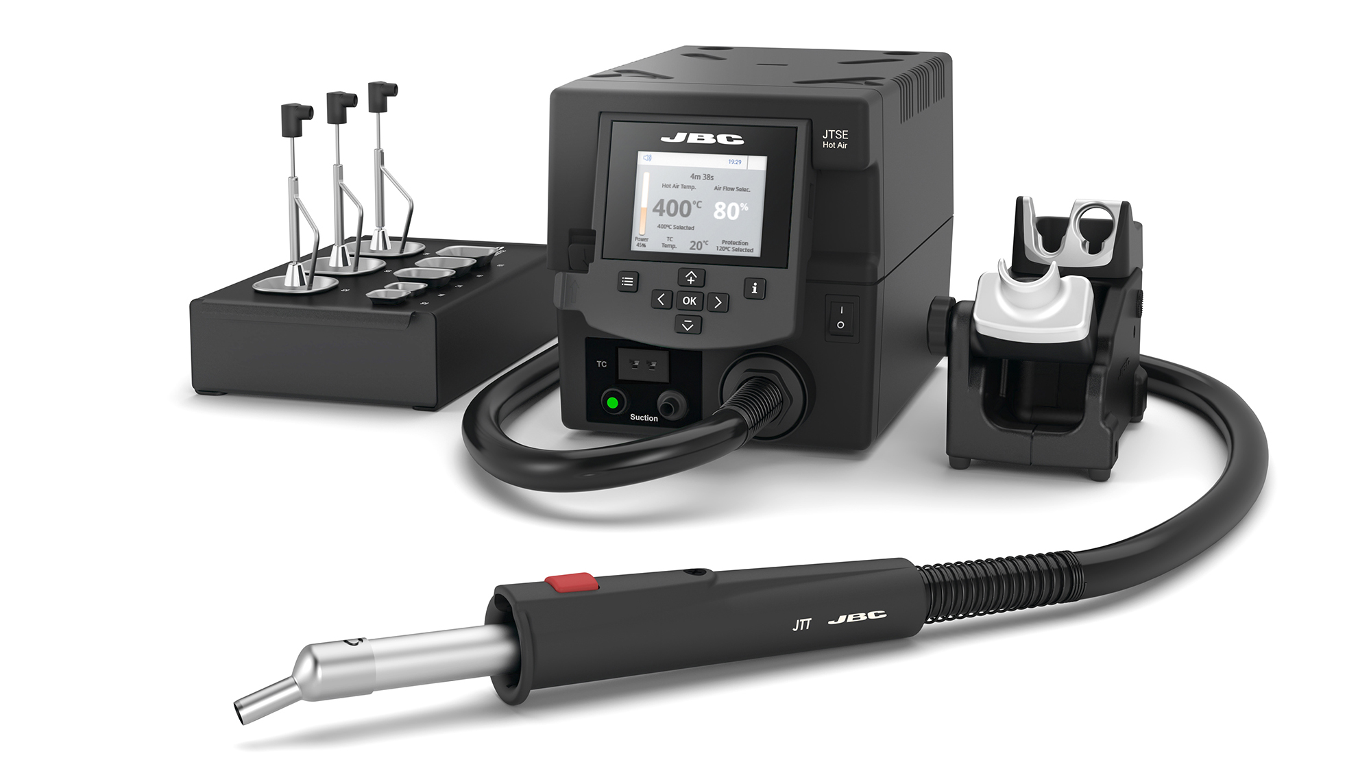
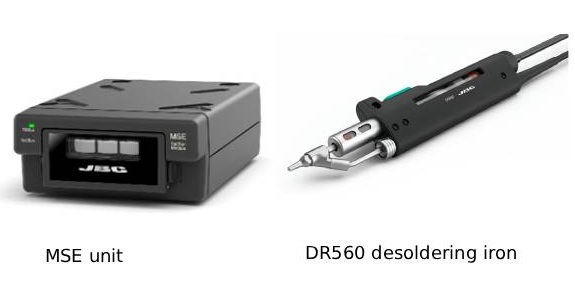
Package-level rework, socket-adapter rework and BGA/QFN replacement on test and load boards require contactless, evenly distributed heat so surrounding fine-pitch components and board materials aren't disturbed. JBC's rework systems combine a soldering iron, hot air station and electric vacuum desoldering module in one controllable setup.
Patient monitors, imaging systems and diagnostic electronics increasingly use BGA, QFN and other fine-pitch packages. JBC's rework systems combine soldering, hot air and vacuum desoldering in one controllable setup, giving contactless, evenly distributed heat that protects surrounding components during rework.
Key applications:
RMSD / RMSE Complete Rework Systems:
Combined soldering, hot air and vacuum desoldering rework station
Contactless rework for BGA, QFN and fine-pitch packages
Test sockets, board-to-board connectors and through-hole components on load boards and fixtures are often mounted for mechanical strength during repeated insertion cycles. JBC desoldering tools clear plated through-holes quickly and safely for socket and connector replacement without pad or via damage.
Semiconductor labs and test-board assembly areas typically operate under strict ESD-control protocols. JBC's stands and tools comply with EC regulations and ESD recommendations, with intelligent stands that cut power automatically when a tool is set down.
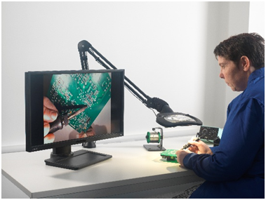
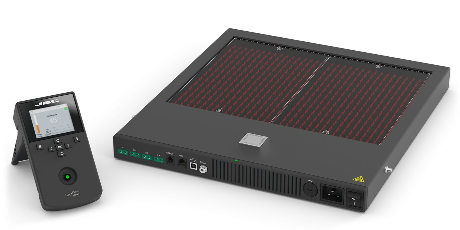
Large test boards, load boards and panelised substrates are prone to thermal shock and warping during localised rework. JBC preheaters bring the whole board to a stable base temperature before rework, while fume extraction protects operators on ESD-controlled lab benches.
Preheaters & Rework Benches
Avoids thermal shock on large multilayer test and load boards during rework
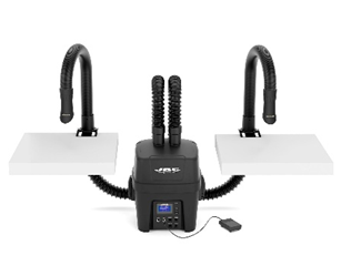
Fume Extractor Kit for 2 Workbenches
Captures solder fumes at source on lab and cleanroom-adjacent benches